Understanding the Depletion Region in PN Junction
The PN junction is a fundamental component of modern electronics. It is the basis for diodes, transistors, and many other electronic devices. The PN junction is formed by bringing together a p-type semiconductor and an n-type semiconductor. When these two materials are joined, a depletion region is formed at the junction. This article will explore the depletion region in PN junctions, its properties, and its impact on device behavior.
What is a Depletion Region?
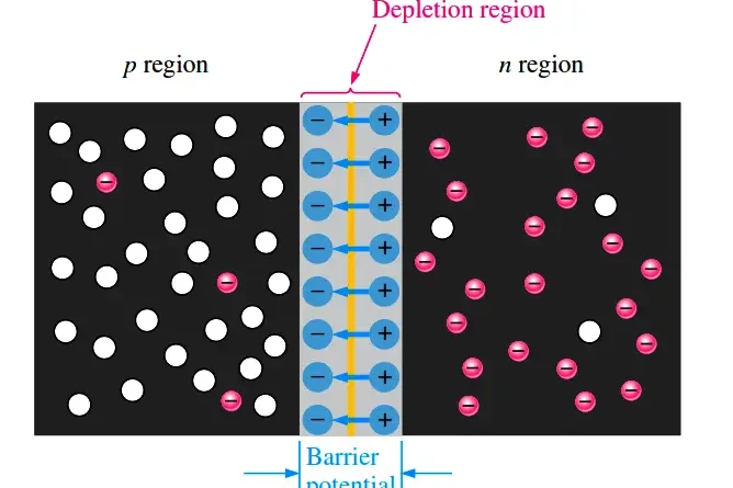
A depletion region is a region in a semiconductor where there are no free charge carriers. In a PN junction, the depletion region is formed at the junction between the p-type and n-type materials. The depletion region is created due to the diffusion of charge carriers from one side of the junction to the other.
In a p-type semiconductor, there are many holes (positively charged carriers) and few electrons (negatively charged carriers). In an n-type semiconductor, there are many electrons and few holes. When the two materials are brought together, the electrons from the n-type material diffuse into the p-type material, and the holes from the p-type material diffuse into the n-type material. This diffusion process continues until there is a balance of charge carriers on both sides of the junction.
As the diffusion process continues, the concentration of charge carriers near the junction decreases. This decrease in carrier concentration leads to a decrease in conductivity near the junction. The region where there are no free charge carriers is called the depletion region.
The Width of the Depletion Region
The width of the depletion region depends on several factors, including the doping concentration of the p-type and n-type materials and the applied voltage across the junction. The doping concentration refers to the number of impurities added to the semiconductor to create either a p-type or n-type material.
When there is no applied voltage across the junction, the width of the depletion region is determined by the doping concentrations of the p-type and n-type materials. The higher the doping concentration, the narrower the depletion region.
When a voltage is applied across the junction, the width of the depletion region changes. If a forward bias voltage is applied (positive voltage on the p-type material and negative voltage on the n-type material), the depletion region becomes narrower. This is because the applied voltage pushes the charge carriers towards the junction, reducing the width of the depletion region.
If a reverse bias voltage is applied (positive voltage on the n-type material and negative voltage on the p-type material), the depletion region becomes wider. This is because the applied voltage pulls the charge carriers away from the junction, increasing the width of the depletion region.
The Electric Field in the Depletion Region
The depletion region has an electric field that points from the p-type material towards the n-type material. This electric field is created due to the separation of charge carriers in the depletion region. The electric field is strongest at the junction and decreases as you move away from the junction.
The strength of the electric field depends on the doping concentrations of the p-type and n-type materials and the width of the depletion region. The higher the doping concentration, the stronger the electric field. The narrower the depletion region, the stronger the electric field.
The electric field in the depletion region has several important effects on device behavior. One effect is that it creates a potential barrier that prevents current flow in one direction. This is why a diode only allows current to flow in one direction. When a forward bias voltage is applied to a diode, it reduces the potential barrier, allowing current to flow. When a reverse bias voltage is applied, it increases the potential barrier, preventing current flow.
The Impact of Depletion Region on Device Performance
The depletion region has a significant impact on the performance of PN junction devices. For example, the width of the depletion region affects the capacitance of the junction. The narrower the depletion region, the higher the capacitance. This is because the depletion region acts as a dielectric material between the p-type and n-type materials.
The depletion region also affects the breakdown voltage of the junction. The breakdown voltage is the voltage at which the junction breaks down and allows current to flow in the reverse direction. The breakdown voltage is determined by the width of the depletion region and the doping concentrations of the p-type and n-type materials. A wider depletion region or higher doping concentrations result in a higher breakdown voltage.
Conclusion
In conclusion, the depletion region is a critical component of PN junction devices. It is created due to the diffusion of charge carriers from one side of the junction to the other. The width of the depletion region depends on several factors, including the doping concentrations of the p-type and n-type materials and the applied voltage across the junction. The electric field in the depletion region creates a potential barrier that prevents current flow in one direction and affects device behavior in several ways. Understanding the properties of the depletion region is essential for designing and analyzing PN junction devices.